Tiny holes are drilled into the pcb assemblers to accommodate component leads and vias for interconnection. These holes are then plated with copper to ensure electrical continuity. The accuracy of drilling and plating is paramount, as any misalignment or defects can result in connection issues, rendering the PCB useless.
Silkscreen Printing: Silkscreen printing is the step that adds labels and identifiers to the PCB. This includes component outlines, reference designators, and other important information for assembly and troubleshooting. It’s essential for ensuring that the PCB is assembled correctly and can be serviced or repaired if necessary.
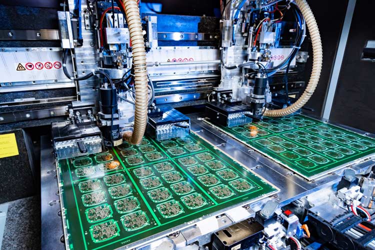
Quality Control and Testing: Throughout the PCB fabrication process, quality control is an ongoing concern. Automated optical inspection (AOI) and other testing methods are used to identify defects, misalignments, or irregularities that may impact the PCB’s functionality. Rigorous testing helps ensure that only reliable and functional PCBs move forward in the manufacturing process.
Conclusion: PCB fabrication is a blend of precision engineering, materials science, and artistic design. It is the foundation upon which our electronic world is built, enabling technological advancements and innovations. With continuous developments in PCB fabrication technology, we can expect smaller, more powerful, and more energy-efficient electronic devices to emerge. As the demand for electronics continues to grow, PCB fabrication remains a critical, dynamic field, offering boundless opportunities for innovation and progress.